Introduction
Registers are in that class of things that you need in order to call a computer a computer by the strict definition of a computer. The word register is a bit of jargon in my opinion. It’s just a fancy term for a small, fast piece of computer memory. That is, in effect, all a register is. Or maybe it’s more correct to say computer memory is just a large, slow group of a bunch of registers. Either way, they’re effectively the same thing conceptually.
Under the hood, however, registers are often implemented different than memory cells. In the Theoputer, the registers are all 74374 chips. These are 8bit (called octal because people love their jargon) D-type flip-flops.
Flippy-Floppies
To understand registers you first have to grab your sunscreen and your flip-flops. A flip-flop, in this context, is an electronic device that can store a binary value (bit) indefinitely until an edge appears on the change signal. A very related cousin of the flip-flop is the latch, which also stores a value indefinitely but the internal bit is changed immediately if the change signal is active. Take the following aesthetically-pleasing circuit:
This is called an SR Latch. The S and R refer to the Set and Reset inputs. What is noteworthy is that this circuit will hold whatever value is in the two NAND gates until the opposite change signal is activated. What we want out of a register is to hold on to a value (like memory) until we choose to set it to something else, but we only want that change to happen during the execute phase of our clock cycle:
We need to latch/store values only when this transition from low-to-high in the clock occurs. For that we need a flippy-floppy. There are several types of flip-flops out there (JK, D, and T being the common ones). Here’s a quick description of each:
- JK: Combines the set/reset functionality of an SR Latch with an input edge signal that triggers the operation.
- D: Simple data bit and an edge signal, where the data will be latched in only on the edge signal transition.
- T: Simple toggle signal bit and an edge signal, where the latched value will toggle when the toggle signal is high and there is an edge signal transition.
What we need is the D Flip Flop! Well, ideally eight of them, because we want to store 8bits at a time in most cases.
The Actual Register
The Theoputer currently uses the same chip for all of its registers, and there are many (10) registers throughout the computer. The specific chip we use is the SN74LV374APWR, which is a TSSOP package LV-series 74*374 “Octal Edge-Triggered D-Type Flip-Flops With 3-State Outputs”. A mouthful, so let’s break that down.
The package refers to the physical dimensions of the chip and its pins. In this case it’s the TSSOP package, which means mere mortals cannot solder it by hand. Well some of us can’t. It’s small. Each pin is 0.19mm wide and the distance between each pin is 0.65mm. That’s small. But that also means the size it takes up on a board is small.
Note: It’s the APWR, and specifically the PWR, of the chip name that indicates it’s TSSOP. Why did they do this?! Why? I have no answers for you. It’s maddening. I’m sure they had their reasons but… sigh.
The LV-series chips are very nice. They are a modern version of some chip families you may have heard about (74LS and 74HC being perhaps the most famous). Internally they are CMOS and must have some crazy engineering because they can operate at 1.7GHz at 5V! Officially the LV stands for “Low Voltage”, but that seems to just refer to the fact that you can run them at low voltage not that they only run at low voltage.
The final piece is the SN74*374. This tells us that the chip is manufactured by Texas Instruments (SN), is part of the 7400 series integrated circuits (most logic gates, etc. will be in this series), and specifically the 374. 374 is like the model number. If you stare at these chip names long enough you’ll start to know that “the 374 is the register”. Of course, specifically, it’s the easy-to-remember “Octal Edge-Triggered D-Type Flip-Flops With 3-State Outputs”. But that’s just a fancy way of saying it has eight D Flip Flops and will keep its contents valid on its outputs unless you tell it to output nothing, which will look like a short circuit / disconnected line (three states: on, off, disconnected).
The Newborn Registry
The earliest versions of the Theoputer register were bulky, but got the job done:
This was also intended to be plugged in to something. There was no Daughter Board back then, so this particular version was only ever used on breadboards to test out the very first ALU. This version also suffered from two design flaws (one major, one minor) that weren’t apparent until the first ISA started coming together.
The Major Flaw
It’s hard to engineer in a vacuum. Vacuums are, well, vacuums. They’re not the real world with all of the dirt and grime and complexity. They’re a nice place to think about solutions, especially scientific ones, but the vacuum’s utility is quickly exhausted because engineers have to build things in the real world.
In the real world of the Theoputer there is a real clock that really pulses between low (0V) and high (5V) voltages. In a vacuum, maybe that’s not the case. Let’s look at the first register design and think about how it would operate in the real world:
Note: This is one of the first schematics I made in this project, and you can see my amateurish skills on full display here.
It may look perfectly fine. Indeed this is the schematic that produced
the assembled board at the beginning of the post and executed
the first operation in the
Theoputer. The problem is the CLK signal. The unsuspecting reader
may not think about the real world pulsing clock and instead think of
the nice vacuum version: a button that a person is pressing to test
out the register. But that pulsing clock is real. And in the design
above every pulse will attempt to set the register.
Imagine a case where the instructions executed are simply:
LAI 0x10
MCA 0x00
The first instruction will work fine. The value \(0x10_{16}\) will be on the data lines, enable will be high, and the read/write signal will be high for a write. The clock will transition from low to high, and bam! The register will contain the value. Now the next instruction. The enable signal is again high, the read/write signal is low for a read. The clock will transition from low to high, and bam! Oh. Well more like bang. At that moment the register will attempt to latch whatever is output from the buffer IBUF1. But that’s a tristate buffer and it’s disabled so there is not a well defined value on the lines going from that buffer to the register. Uh oh. Here’s a not-great attempt to model this:
Again the problem is that we only want to latch data into the register when the clock goes from low to high AND the register is enabled. The original design completely missed that point. Not only that, if we were to use the scheme of having an enable signal and a single read/write signal, we would have to perform some complex logic to see if the register was enabled AND the the clock transitioned AND the operation was a write. So maybe the enable and read/write pair are not great. Turns out they’re not great. And not just for this major flaw reason.
The Minor Flaw
The minor flaw with the original register is subtle. Let’s look at its schematic again:
There are two buffers handling the connection from/to the
databus, the register itself, LEDs for
each bit, some decoupling capacitors to reduce ground noise, and some inverters. Right away it’s probably
notable that we have inverters here. That adds an extra chip for what?
In the schematic there are two control lines: EN and R/W. So
the idea is to enable the register and set what kind of operation to
perform. This alludes to the problem.
Imagine what the following instructions would imply:
LAI 0x10
MCA 0x00
The first instruction is a loading instruction and thus we would need
to set the controls EN high and R/W high. Ok maybe our
instruction decoder emits high signals on the control lines. Then we
can do away with inverters, simplifying our design, and reducing the
bill of materials (BOM). But now consider the MCA 0x00
instruction. This is a read and thus we need to set EN high and
RW low. Well now we need that inverter again. And it’s not hard
to see that no matter what, if we have this enable signal and a
read/write signal in one, we will always need an inverter.
This is poor design, but it’s hard to appreciate it until you think through how the register will actually be used in the computer. The solution is fairly straightforward. We just want to control read/write operations on the register with either all high signals or all low signals. The second register design already solved both the major flaw and the minor one:
Here we’ve eschewed an enable signal and a read/write signal and just
combined them into a much better pair: IN and OUT. But
it’s instructive to see why this new pair is better and we learn best
from screwing the proverbial pooch.
We Need a Montage
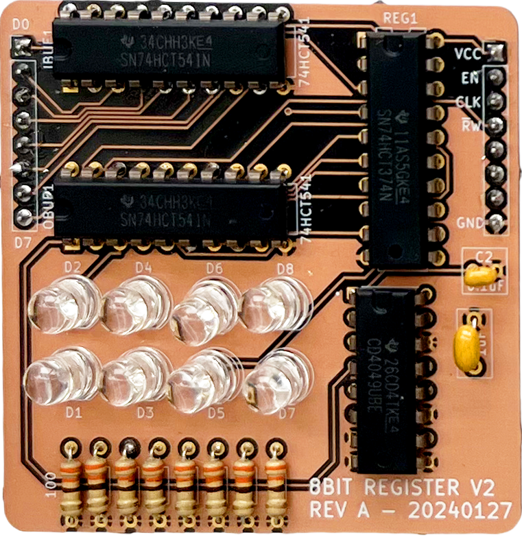
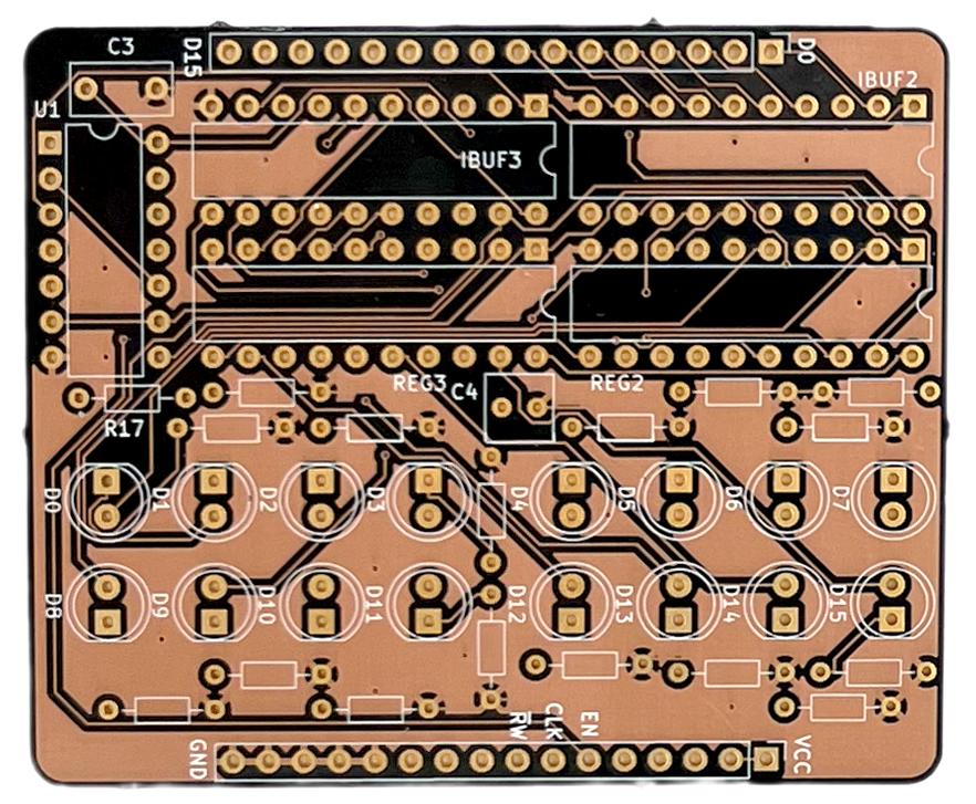
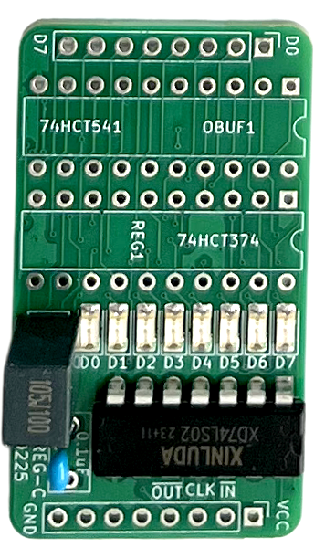
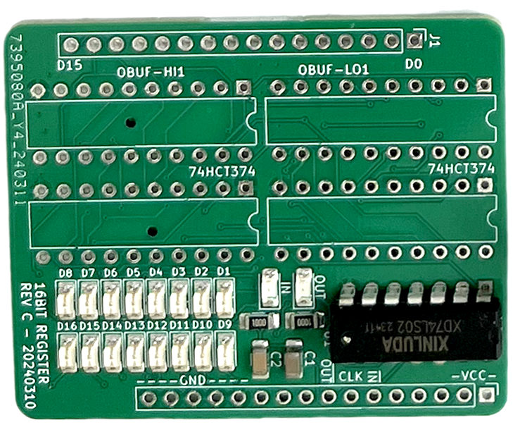
Here are some nice photos of the register (both 16bit and 8bit) as it grew up from a flawed POS to a sleek non-pluggable dude:
Why Bother?
Apparently memory and registers are basically the same thing, so why bother having registers at all? The slow vs. fast difference between the two types of temporary storage is very important and relevant for the computer you’re reading this post on. But that’s probably not a Theoputer.
In all honesty the Theoputer is quite slow by today’s standards. At the speed it operates fastest (1.8432MHz) there’s truly no real difference between memory access times and register access times. That could change some day if the clock speed of the Theoputer can ever get above the read/write delays in the current RAM chip (a IS61C6416AL-12TLI), but that seems pretty unlikely given those read/write access times are both 12ns or ~83MHz!
So why bother? Two reasons:
- The goal here is to build a computer, and computers fundamentally have registers
- Registers make it much easier to see and understand what’s happening
The first point might seem gratuitous, but recall we need to eventually write an assembler and probably a compiler for the Theoputer. When we go to do that it will be more familiar to have the notion of registers. Again, it’s not necessary, but it can help.
The second point there is probably the real reason the Theoputer still has registers. Trying to debug memory is extremely challenging. By having registers around it’s trivial to put a value into one of them, halt the computer, and look at what’s in the register. This is made even easier by having diagnostic LEDs that are attached to each bit of every CPU register.