Introduction
This is more of a beach head than anything. The “Daughter Board” is very complex and contains a considerable amount of the actual “CPU”, so a single post about it isn’t really feasible. This should just serve as more of a tour around the board itself, with pointers to the individual parts in much more detail.
I’ll also take this moment to share a fun note. One of the tenets I’ve tried to adhere to in designing and building the Theoputer is to limit outside help. It’s not so much that I don’t want/like help, but more a way to see if I could figure things out on my own. I am, after all, officially an “expert” of Computer Science and in my hubris have a small inkling that I could discover something interesting because I lack the curse of knowledge in this case.
So far, nothing novel. However! The name of this board is a funny situation. When I was designing the earliest parts of the Theoputer I knew that I need to work incrementally and modularly. The 8Bit Register and the ALU were two of the first boards I ever made, but I quickly needed a way to connect them. I thought to myself:
"Self. You have these little boards, like little daughters. Plug
them into a larger board that contains them. Clearly called the
Daughter Board!"
It took me a good year before it dawned on me that I had “re-invented” the Motherboard, but missed the now-obvious relationship between daughters and mothers. Alas. I’ll chalk it up to my own daughter not having been born until after I coined the term.
A Tour Around the Board
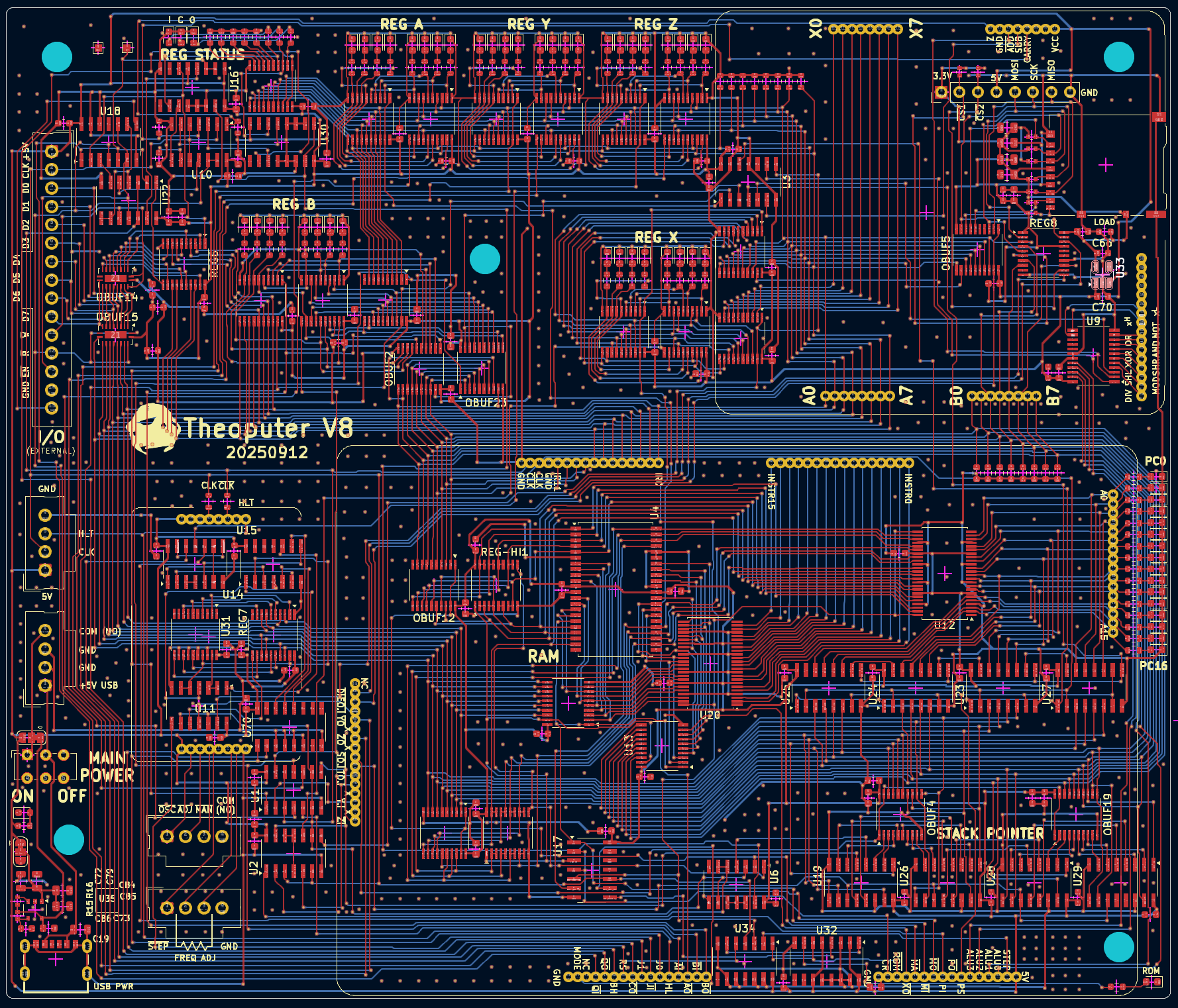
Here is the current version of the Daughter Board:
That’s a lot, and it doesn’t even really tell the full story, because the entire point of (incorrectly) naming this thing a “daughter” board is that there are other boards that plug into it! It’s probably very hard to even see the outlines of those boards from the complex viewer above. So let’s simplify things a bit and just look at the pieces:
This view just shows the outlines of the boards, the chips on the Daughter Board, and a few pieces of information that will end up being printed onto the printed circuit board during fabrication.
There are twelve sections we will look at briefly, with pointers to more in-depth considerations:
- Data Bus
- Registers
- Clock
- Program Counter
- ALU
- Branch Control
- Instruction and Control
- I/O
- Power
- RAM
- Stack Pointer
- SD Card
Before we look at each of the sections, just take a mental note that every single chip on the board has at least one 0.1uF capacitor right next to its VCC pad. Some have an additional 1uF capacitor. These are decoupling capacitors and are critical to ensuring the board is light on ground noise, which is a much deeper concept worth reading about at your leisure.
Data Bus
The data bus isn’t really a section of the board because it is a group
of traces that go all over the board. Fundamental to the operation of
the Theoputer is the concept that data of any form is “put onto” and
“read from” a single group of 16 wires. By controlling which other
parts of the Theoputer are either reading or writing to/from these 16
wires we are able to perform nearly all of the operations of the
CPU. Here are those lines, DBUS0 through DBUS15, crossing the
board on the bottom layer (blue):
You can read more about what the data bus is and why it’s important in
the data bus post, but for now just note
that it goes everywhere! Connecting up all the things that need to
speak to each other, and with 16bits of data. It’s worth also noting
that the data bus is often considered as two separate buses, a “low”
8bit bus comprised of the lines DBUS0 through DBUS7 and a
“high” 8bit bus comprised of lines DBUS8 through DBUS15.
The only other thing worth mentioning here is that every connection to the data bus has an electrical component called a buffer, and ever connection from the data bus has another buffer. These buffers are like electrically-controllable breakers, so that if the buffer is disabled, it’s as if there is a disconnected wire between the bus and whatever is on the other side of the buffer. This ensures that only one thing ever writes to the data bus at a time. That’s important because if there were a scenario where two things tried to drive the data bus lines at the same time, we would have a phenomenon called bus contention, and bus contention makes circuits very unstable.
Registers
There are actually several “kinds” of registers on the Theoputer, but this section is dedicated to the “CPU registers”. If you’ve studied or used other CPUs at a low level this concept will be straightforward. If not, a register is a jargon-y word for a circuit that can store a value indefinitely, until you decide you want to store a different value. Very similar to “memory”, but usually much faster although in the Theoputer case the speed difference doesn’t currently matter.
The post about Registers contains a lot of the details about how registers work on a low-level and how they work at a high-level in the Theoputer. But for the tour, the main takeaway is that there are four “general purpose” CPU registers, an ALU register, and a CPU status register.
Registers A, B, Y, and Z
Registers A, B, Y, and Z are general purpose in the sense that they are controllable by a programmer. You can write and read to these registers freely, e.g. via the instruction LAI 0x3A which Loads A with an Immediate byte value \(\textrm{3A}_{16}\). Registers A and B have been around in the Theoputer since its inception, while Y and Z were added in version three.
The only notable difference between these registers is that Register B
is the only register that can address, and be addressed (as of V7+),
the upper eight data bus lines DBUS8 through DBUS15. This
ability is critical to certain instructions that need to read/write
the “high” byte on the data bus.
ALU Register: X
ALU operations produce 8bit values that are stored in Register X after
any ALU operation. Only the ALU can write to this special register,
but it can be read from “normally” in the sense that there is a read
signal (XO) that will cause the contents of Register X to be put
on the low byte of the data bus (i.e. lines DBUS0 through
DBUS7). There is a little bit of extra gate logic to get this work
correctly:
If you follow the logic you’ll see that Register X is only written to
during an ALU operation (on the ↑CLK signal as always) and can
only be read from onto the data bus low byte lines.
Note: If the NOR gate with an inverted
CLKsignal as theCpinput signal on the register is unintuitive/confusing at first glance, checkout Registers to see the details for why that makes sense.
CPU Status Register
The CPU status register is similar to Register X in that it cannot be written to by programmers, but can be read from. Its purpose is to, well, contain information about the status of the CPU. At first that might seem like a weird thing to need/do, but the kind of status that it captures is critical to certain operations. Here’s the schematic of it:
You can see that it only captures three bits of data:
- The state of the signal
ALU_OFLOW - The state of the signal
ALU_CARRY - The state of the signal
INT_0
It turns out that the last signal INT_0 isn’t even implemented so
it’s only two bits! But those are critical bits of information,
containing the last status of the ALU since clearing the status
register via CR. And those two bits are necessary to deal with
ALU subtraction and general
overflow conditions of the ALU.
Note: Getting this simple register to work correctly has been a journey that I’ve not enjoyed at times. I went back and forth on ways to implement the ALU statuses, etc. that would avoid having a dedicated reset signal and instruction but eventually had to acquiesce because all my other strategies created breaking bugs.
Clock
The clock is one of the three remaining boards that plug into the Theoputer daughter board. You can see the outline of the most-recent version of the clock in the daughter board here:
The clock itself is small but mighty. It’s also one of the few analog-like circuits in the entire computer, so while it is physically small it’s rather complex. There are several posts about how the clock works, starting with an overview of some clock basics.
The interface to the clock board used to be very simple, consisting
only of the the CLK and CLK as output signals (180° out
of phase) and HLT as an input signal.
To facilitate external controls of the clock speed and type (manual step, adjustable, and built-in 1.8432MHz oscillator) there are now some pins at the bottom of the board that connect to fancy plugs/headers on the daugher board itself.
The only other thing worth noting here are the two resistors near the
top of the board, right by the CLK and CLK labels. These are
the transmission line source resistors we needed to add after
discovering that the clock lines were action like
tranmission lines.
Program Counter
The program counter is very crucial to the operation of the Theoputer and almost every CPU out there. Maybe every CPU out there. Its job is to keep track of where in the instruction list (program) the CPU currently is located. So if you have a list of three instructions to execute like:
LAX
JPA
HLT
The program counter will start at 0, then increase to 1, and finally 2 before the HLT instruction halts execution. This is a great time to recall the role of the clock in the Theoputer. Its job is to cause “the next thing to happen” and one of the ways the clock does that is by advancing the program counter! It’s not exactly that simple because the clock also needs to advance the microcoder (see the Instruction and Control section for a bit more on that).
The program counter isn’t much more than a 16bit register (oh look! another kind of register) with some special control lines to make it easy to increment it by one and to set it to a specific value:
Notably this is a 16bit register, comprised of four separate
“synchronous counters”. There’s more detail on this in the post about
the Program Counter, so for now
the most important thing to note is that there are two input control
signals: PI, and PS. (Note: CLR isn’t currently
used). PS is set high whenever you want to perform a Program
counter Step operation and PI is set high for a Program
counter Input operation, which uses all 16 DBUS lines to set
the program counter.
To give a brief preview of how this typically works, consider the prior three instructions again:
LAX
JPA
HLT
While there is no actual microcoder assembly language, we could look at these three instructions in a fake microcoder language as:
;; LAX (PC = 0)
XO, AI
PS
;; JPA (PC = 1)
AO, PI
;; HLT (PC = RegA)
HLT
You can see from above that after many instructions we set the PS
signal active indicating to the CPU to go to the next instruction in
order. However, jump-like operations directly set the program counter
to indicate to the CPU that the next instruction is at a specific
address. In the contrived case above you’ll have to put on your
imagination creation hat and assume that the contents of Register X
were 2.
I/O
Even on the first fully-assembled Theoputer there was I/O! That may seem like an overreach, but how else can you expect to speak to the rest of the world without some I/O. The I/O system has also moved around the most, but is currently nestled in the top left part of the board:
That is both the set of chips that make the I/O go and the actual plug/headers/port itself. Hey look! Another register:
The I/O interface is a bit complicated. There is a fairly intricate dance that has to take place to ensure that only I (input) or O (output) is happening at one time and to ensure that data that is outbound stays valid long enough for whatever is outside the CPU to read it. There’s also a bit of signaling that is available to I/O devices that tells them when it’s safe to read/write to help coordinate everything. As usual, the post about the I/O Interface is a better place to learn the details.
At a high level the I/O interface is intended to “look” like another
register to the CPU. All of those gates and that register are there to
give the illusion that this is just like Register A. Of course that’s
not true and if the I/O device is quite slow then it will not operate
timing-wise like Register A, but reading/writing does work exactly the
same way. As you can see there are the usual DBUS0 through
DBUS7 data bus lines, a couple buffers to ensure only input or
output is happening, and there is a register to hold on to the output
data until another output operation (via QI) is encountered.
ALU
If there is a “brain” of the CPU then it’s probably safe to say that’s the Arithmetic Logic Unit (ALU). Typically if you’re using a computer you want it to compute something and typically that computation will involve an operation handled by the ALU. Here are things that the Theoputer currently can compute:
- Addition
- Subtraction
- Bit Shift (Left and Right)
- Bitwise AND
- Bitwise XOR
All of the operations work on 8bit inputs, which as usual come from
the DBUS lines.
On this grand tour of the daughter board, the ALU is one of the more special stops because it is one of the few remaining actual boards that is plugged in to the daughter board. You can see the headers where that happens in the top right corner of the daughter board:
Here you can see the two input bytes labeled A0 - A7 and B0 - B7. The
signals connected to these inputs are DBUS0-DBUS7 and
DBUS8-DBUS15 respectively. Here you can see that we are using
the 16bit-wide data bus to our advantage so that we don’t need to
individually load each byte to operate on before performing the
operation. That decision comes at a cost though because it means two
things:
- We need to support 16 data buses, which is more lines to manage
- We need to have some way to read/write to the bottom/top bytes of the data bus independently
That last point is why Register B has the
special property that it can read/write from/to the
DBUS8-DBUS15 lines.
Also noteworthy about the ALU interface are the X0 - X7 connections. Recall that there is a special ALU output register (Register X) that holds on to the last ALU operation. Those X lines connect to that register, which itself is actually on the daughter board not on the ALU board:
It’s a bit challenging to follow the traces but you should see that the X outputs from the ALU board connect to the REG X block.
Branch Control
At first it may seem odd to have a section dedicated to branch control, but it turns out that supporting branches isn’t as trivial as just reusing other parts of the Theoputer. If you’re familiar with modern CPU architectures you may be inclined to think that this section has something to do with branch prediction, but it does not! That is a much more complex feature of CPUs that is important only when dealing with super scalar architecture, and the Theoputer is a regular old scalar CPU as discussed in the post about the Clock.
On the most-recent versions of the daughter board the branch control logic isn’t labeled, but it is all grouped in the same area under the Clock board:
That’s not very instructive on how the branch control works, so let’s look at the schematic:
Here we see there is a register (ahoy there!), connected to a chip that outputs if that register contains zero, and a few inputs:
OP0andOP1which control the type of branching as a 2bit number:- 1: X == 0
- 2: X >= 0
- 3: x < 0
X0throughX7which is labeled vestigially incorrect and actually connects toDBUS0throughDBUS7PIwhich you may recall from the Program Counter section and is a control signal dictating that the CPU should set the program counter to the value on theDBUSlines.
There are some oddities you may note in the list above. For specifics, refer to the more in-depth post on the Branch Control.
Instruction and Control
This one is a doozy (spelling?). It’s by far the most complex section of the Theoputer save for maybe the daughter board itself. There are several posts about this section, which is actually one of the three remaining plug-in boards to the daughter board. Start off on the introduction post about the Instruction and Control board to go deep on that.
For now, we can see how the Instuction and Control (I&C) board interfaces with the daughter board and thus the rest of the Theoputer:
That large outline is where the I&C board plugs in, and as you can (hopefully) see, there are six separate headers each of which is 16pins! That’s a lotta pins. Not every pin is used, although most are. At this small 1.27m pitch (distance between pins) it’s far easier to source the correct headers when they’re all the same length. They are, somewhat unfortunately, too small to get strong-enough pins that can be broken to the correct length.
Let’s look at the schematic here too because this is another case where that’s helpful:
That certainly is easier to see, but that’s still a lot of lines! Let’s just go over some of the big groups:
PC0throughPC15: The 16bit program counter value as an inputINST0throughINST15: The 16bit wide instruction inputIR0throughIR11: The instruction register (oh haiii) output connected to the bottom 12bits of theDBUSlines- A bunch of control lines like
AIandAOthat are used to control register input/output modes respectively. CR: Used to reset the CPU Status Register to 0SO,SI,SP_DECR, andSP_INCR: Used to control/use the stack pointer via an output signal, input signal, and an increment or decrement signal respectively.BO_HI: Used to control Register B’s read/write to the high data bus byte onDBUS8throughDBUS15versus the usual lower byte onDBUS0throughDBUS7.RS: The global reset signal, intended to be used by various systems to reset themselves to the “start” of execution.J0andJ1: Connected to theOP0andOP1of the branch control system to choose which kind of branching operation to perform.HL: The global halt signal, which stops the clock output effectively halting the system.MA: Used to control whether the memory address register should be read fromDBUS.PI: Used to control whether the program counter should be set from theDBUSlines.PS: Used to control whether the program counter should be incremented (stepped).ALU0throughALU3: Used to control which ALU operation should be performed.STEP: An output from the I&C board indicating that on the next↓CLKthere will be a step-like operation (i.e. the program counter will change).EXEC_MODE_RAM: An output signal that indicates whether instructions should be fetched and executed from RAM (high) or from ROM (low).ROM: An input signal that allows the other Theoputer systems to indicate that the I&C board should enable (low) or disable (high) the ROM chips.
Phew. That’s a lot. Probably enough for this entire section, so let’s leave it at that for now and if you want to read more of the details check out that beach head post on the Instruction and Control board.
Power
Providing power should be easier right? Haha! Think again. Nothing’s
easy in the land of electrons! Well it can be easy and in fact for
many versions was just a USB-C port connected directly to the main
VCC power line. That changed between V6 and V7 whereupon the power
system got an upgrade to be more robust:
There’s fairly clearly an ON/OFF switch and a USB-C port at the bottom. But in between those two components is a bunch of capacitors (to help with power delivery during high-load spikes) and a chip that’s hard to see in the board view, but easier to see in the schematic:
That chip is the NCP380HSN05AAT1G, which is a power switch used very frequently in USB hubs. In this case, the specific chip has a fixed output current of 0.5A, which is currently (pun intended) enough for the Theoputer. Notably, this chip does not handle the USB 3.* (which is synonymous with USB-C) power negotiation protocol, so it has to be plugged in to a USB-A port on the providing end.
RAM
Originally RAM was only used in the Theoputer as a place where programs could store and retrieve data to/from. Much like the computers of yore it became clear, eventually, that using RAM to also be able to store instructions was a game changer. At that moment, the RAM system became a lot more complicated.
It’s hard to show on the board where RAM is nowadays with this added complexity, but it’s roughly here:
Without diving into the internals of how the RAM system works (that you can find in the dedicated RAM post), here’s the schematic of the daugher board interface to it:
The gates and the JK flip-flop are there to help coordinate the handoff between executing instructions from ROM (the default) to executing them from RAM. There is a dedicated post to that upgrade as well, describing how the Theoputer executes RAM instructions.
For now the important things to note are that there are a set of
control lines that determine whether RAM should output its contents to
the INST{0-15} instruction bus (ROM, EXEC_MODE_RAM, and
STEP) and there are a set of control lines for the memory itself
to control the address to operate on (MA) and whether the
operation is an input (MI) or an output (MO).
Stack Pointer
This is one of those sections that you learn about in some course about programming or assembly or computer architecture. Assuming you’ve gone through the pedagogy, the idea of a stack pointer (or at least a “stack”) will not be foreign. But does it make sense why this is important? The earlier versions of the Theoputer didn’t have a dedicated stack pointer and they worked just fine. Well fine enough.
But without a dedicated stack pointer, you would inevitably discover why dedicated stack pointers are incredibly useful. There are, of course, more details in the post about the Theoputer Stack Pointer, so you’ll have to convince yourself or read that post to understand why the Theoputer dedicates a fairly sizeable portion of the board to it:
In the section describing the Instruction and Control signals there are details about the signals that control the stack pointer, but here they are again for posterity:
SO,SI,SP_DECR, andSP_INCR: Used to control/use the stack pointer via an output signal, input signal, and an increment or decrement signal respectively.
SD Card
This is the newest part of the Theoputer and it’s not even be validated as working as of writing this! SD Cards have their own protocols (some of which are now proprietary) and all of which operate at voltage levels below the Theoputer’s 5V. So much of the SD Card area is occupied by power regulation:
Once again that’s likely hard to understand, and once again there is a dedicated post about the SD Card Interface and once again the schematic is potentially more useful:
Here we see the voltage regulator (MIC5504-3.3YM5) responsible for converting the 5V VCC power rail into a stable (we hope) 3.3V needed by the SD Card Protocol. There are also several capacitors to help with current spikes, which are fairly likely in this case when the card is inserted.
Apart from that the SD Card interface works very similarly to the
generic I/O Interface, with a register (howdy there!) for
keeping output data valid for as long as we need and a buffer to the
DBUS lines to handle bus contention.
One unique thing about the SD Card Protocol is that it is actually a serial protocol. That’s actually a lot more common for peripheral protocols in computers than a parallel protocol, but the Theoputer is more of a parallel-leaning entity. This because of the 8bit nature of the computer. We always want to operate on 8bits at a time, which is similar to saying we want to work on 8bits in parallel. In some cases we even use 16bits (e.g. the memory address register) but we certainly don’t send one bit at a time between parts of the system.
There are a number of ways to convert parallel-like signals into
serial-like signals. In the case of the SD Card interface we are using
one of the simplest: just use a single bit at a time!. That’s why
there input to the first bit of the register (D0) is DBUS0,
which in turn is connected to SD_SPI_MOSI - the SD Card serial
input line.
You’ll notice four additional lines coming out of the Theoputer and into the SD Card:
SD_SPI_CLK: Used as the clocking signal for the SD Card and any other SPI-compatible peripheral that’s connected to the Theoputer.SD_SPI_CS: Used to indicate to the SD Card that it is the peripheral that should read the serial data (SD_SPI_MOSI) and serial clock (SD_SPI_CLK) lines.SPI_CS1: Used to indicate to a second SPI-compatible peripheral that it should handle the serial data and serial clock lines.SPI_CS2: Used to indicate to a third SPI-compatible peripheral that it should handle the serial data and serial clock lines.
You may see something interesting in the information above. In the Theoputer, SD Cards are communicated to via something called the Serial Peripheral Interface protocol. This is a fairly standard protocol that many peripherals use and the Theoputer has some extra headers and pins to allow for other SPI peripherals to be connected.
Finally, there are some lines coming out of the SD Card and into the Theoputer:
SD_SPI_CS: Same signal as above, just as a helpful output to the computer.SD_SPI_CLK: Same signal as above, just as a helpful output to the computer.SD_SPI_MISO: The serial data line out from the SD card (or any other connected SPI peripheral) and into the TheoputerSD_DAT1: SD Card signal line that is used for advanced operations currently not implemented.SD_DAT2: SD Card signal line that is used for advanced operations currently not implemented.SD_CD_B: A signal coming from the physical SD Card slot that asserts high when an SD Card is inserted.
Wrap-Up
Phew! That was a lot of information. This post will probably serve as more of a reference (to me) than anything. It seems like there enough detail to sort of understand what’s going on, but not nearly enough detail to put it all together into a cohesive understanding.
If nothing else it was helpful to organize my own thoughts about the different systems in the computer, so there’s always that!