What is the Theoputer?
The Theoputer is a Turing-complete computation device. That means it can do everything that you can do on the computer you’re reading this from. It’s slower, but it is just as capable given enough time.
I built this computer from scratch, where scratch means from logic gates available in Integrated Circuit packages. I designed the schematics, the printed circuit boards, the instruction set architecture, the simulator, and the C compiler. I had some help, but for the most part I tried to avoid reading too much about how to build such a device so that I could learn by doing.
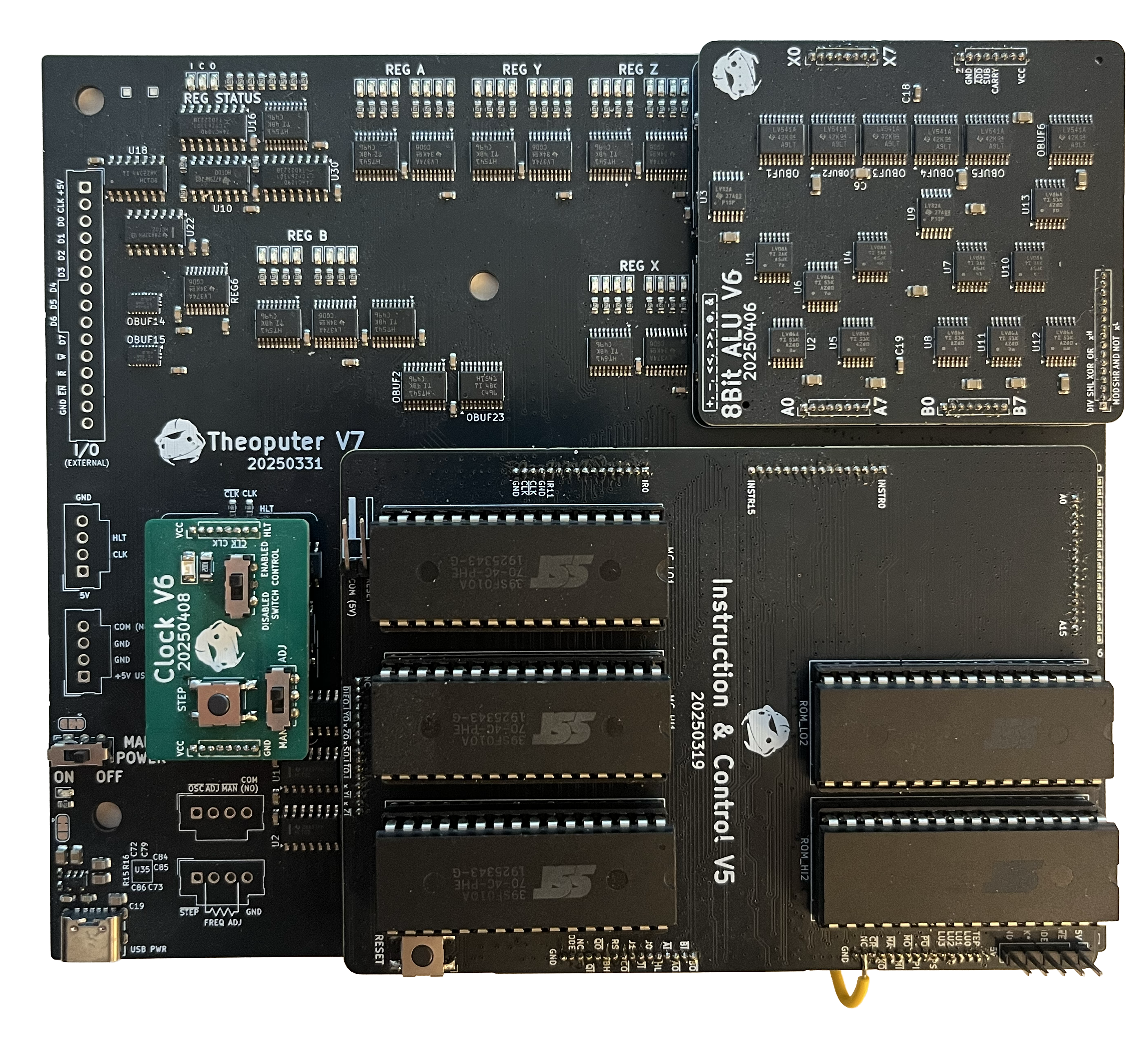
Currently there are four printed circuit boards that combine to make the full Theoputer (named after my son Theo):
Here is all of that assembled:
How Does It Compute?
Like most computers the Theoputer is driven by a clock circuit that
produces a square wave output. This clock signal (CLK) and its
inverse (CLK) are used to define the two halves of the (fetch
and decode) + execute cycle:

Fetch and Decode
As soon as the CLK signal goes high (which indicates the CLK
signal is low) a new (fetch and decode) operation happens. At this
moment the program counter is used to address the program ROMs and the
value across the two ROMs (i.e. a 16bit value) is latched into the
instruction register. This is, effectively, the fetch operation.
Before we discuss the decode operation, it’s important to know that the Theoputer uses microcode instructions. A single instruction like “load the value \(\textrm{0x10}_{16}\) into register A” (i.e. LAI 0x10) is actually comprised of two micro-instructions:
- Put the value \(\textrm{0x10}_{16}\) on the databus and set register A to read mode
- Advance the program counter by 1
The Theoputer knows how to decode LAI 0x10 into that set of micro-instructions by way of three microcoder ROMs on the Instruction and Control board:
Those three ROM chips get flashed with data in such a way that the instruction LAI 0x10 maps to those two micro-instructions.
By way of example, the row in ISA 5.1 for LAI 0x10 (Load A w/ immediate) says the opcode is:
$$ 0 1 1 0 0 0 0 0 (\textrm{I}_{08}) (\textrm{I}_{07}) (\textrm{I}_{06}) (\textrm{I}_{05}) (\textrm{I}_{04}) (\textrm{I}_{03}) (\textrm{I}_{02}) (\textrm{I}_{01}) $$That’s 16bits long, with the last 8bits indicating that the opcode contains 8bits of data at the end. All instruction opcodes in the Theoputer are 16bits long but only the most-significant 8bits are used to map to micro-instructions. The bottom 8bits are always placed into an instruction register that can be enabled or disabled to output to the databus.
The top 8bits (\(0 1 1 0 0 0 0 0\) in this case) are the actual
opcode. That 8bit number translates to the 16bit decimal number
\(24576_{10}\) if we ignore the bottom 8bits and treat them as
zeros. This number is used as an address in the three microcoder
ROMs (the same address across all three). At that address you would
find a 24bit number – 8bits for each of the three microder ROMs. The
value at \(24576_{10}\) will set the control signals IO
(instruction register output) and AI (register A input), and the
value at \(24577_{10}\) will set the control signal PS (program
counter step).
Every CLK pulse advances the microcoder stepper by one. On program
counter operations, the microcoder is reset back to zero so the next
instruction can be latched based on the new program counter value.
Execute
After the fetch and decode stage, there will be a set of control lines
in the Theoputer that are active (notably most of these lines are
active low). On the transition of the CLK (notice this is
NOT the inverted clock this time) from low to high, actions
happen. Actions are anything that changes the state of the computer in
any way. Or, if it’s easier, actions are everything that’s not a
control signal changing.
One of the more common actions is to change the value inside a register. Have a look at the interface to one of the registers in the schematic for the daughter board:
That NOR gate is doing the duty of handling the read control signal
(AI) and ensuring the value of the register is set only during
the low to high transition of the clock. Check the truth table for
yourself:
| Cp | |||
|---|---|---|---|
| 0(↓) | 1 (↑) | 0 | 1(↑) |
| 0(↓) | 1 (↑) | 1 | 0 |
| 1 | 0 | 0 | 0 |
| 1 | 0 | 1 | 0 |
If you look around the schematic (which you can do using the viewer above) you’ll see that any time state is changing there is some form of that same logical pattern ensuring the correct read/write signal is set and the clock is transitioning from low to high.
How Is It Programmed?
A computer needs something to execute or it doesn’t compute. Trees falling the woods making sounds kind of thing there.
In the Theoputer most programs are created on a normal computer and then flashed/written to the two program ROMs that are plugged into the Instruction and Control board:

Note: These used to have nice quick-release sockets, but they take up a lot of space and there is a now a direct programming/debugging board that plugs into these save sockets allowing for direct programming of the computer.
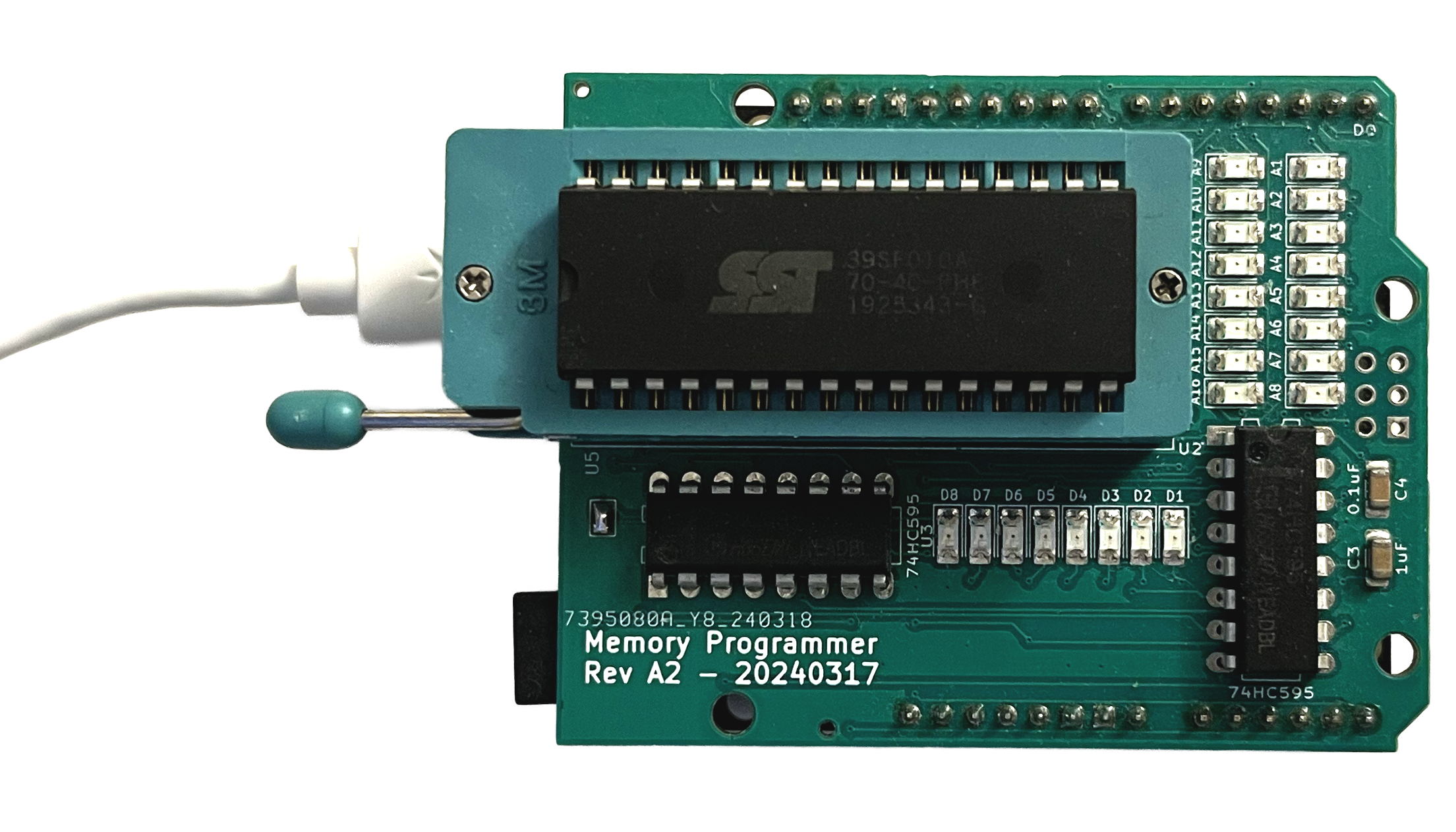
You can write programs in either Theoputer Assembly or Theoputer C (which is pretty close to regular C) using the simulator, and then write the programs to the program ROMs via the built-in programmer in the simulator. There is a companion board called the ROM Programmer that allows you to individually insert the program ROM chips and program them via a USB cable with the simulator:
Closing Thoughts
That’s a pretty high-level overview of how the Theoputer works. It is, despite its homemadeness, quite complex and doesn’t lend itself well to this kind of discussion. But it may be the description that causes you to read more. Fingers crossed.