Introduction
The way I was taught about how computers work was via the “fetch, decode, execute” loop. I have no idea if this is standard pedagogy, but I imagine it is. The idea is that any computer must have a process to figure out the next operation to perform (fetch), it needs to be able to turn that operation into the correct set of control signals (decode), and of course once all of those control signals are setup it needs to actually perform the operation (execute).
I’m sure there are computers out there that think of these three steps as independent, and it’s probably the case that most are like that, but in the Theoputer I decided to simplify things a bit. Instead of three steps, I decided to combine the (fetch and decode) steps into a single step.
The reason for this is really about the clock! The clock has two distinct phases: the down phase and the up phase. Trying to split things into threes or spending three clock cycles for each instruction just seemed like a waste.
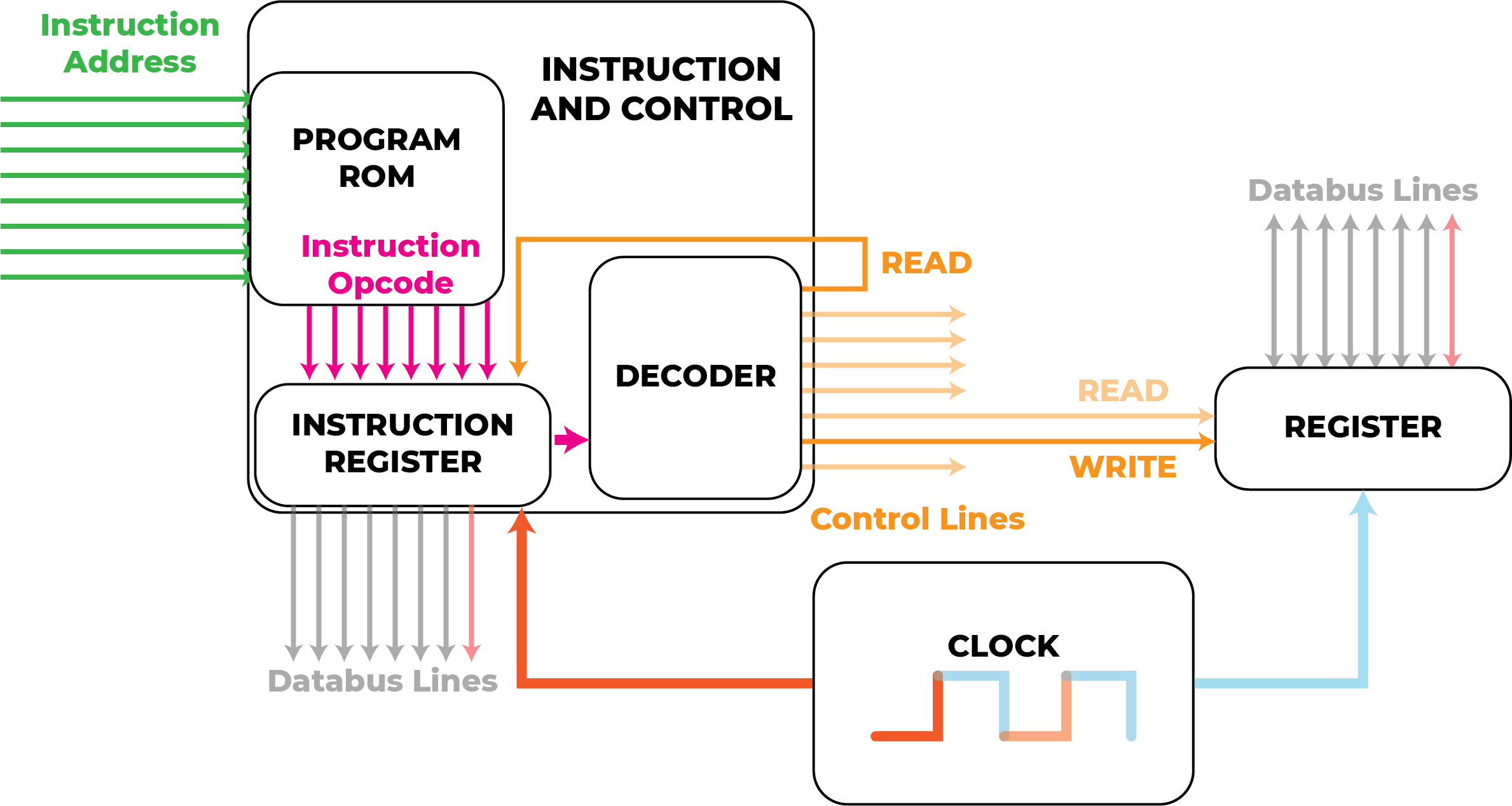
The circuit responsible for this combined fetch + decode stage I have dubbed the Instruction and Control board. Its job is to fetch instructions and decode those instructions into the set of control signals.
And it is a board. One of the few (down to three as of writing) circuits/boards that are plugged in to the Daughter Board. It’s also one of the more complex parts of the Theoputer apart from the Daughter Board, and it is the largest board that’s plugged into the Daughter Board. This post will be about the current board, which doesn’t suffer from the many issues that the prior boards plagued me with, but I will try to walk through some of the stickier parts along the way.
Two Clock Phases, One Set of Lines
Recall that when we designed our clock we made a point about how there are two phases:

The Instruction and Control (I&C) circuit is only responsible for that first phase, labeled the “fetch” phase. The I&C board is also the only circuit that is allowed to operate in this fetch phase because it is uniquely responsible for setting the control signals in the Theoputer. We discussed this a bit in the overview of how the Theoputer computes, but let’s do a slightly deeper dive.
Simplified Model
Let’s avoid looking at the schematic for now; it’s a bit complicated for our purposes. Instead, consider the following blocks:
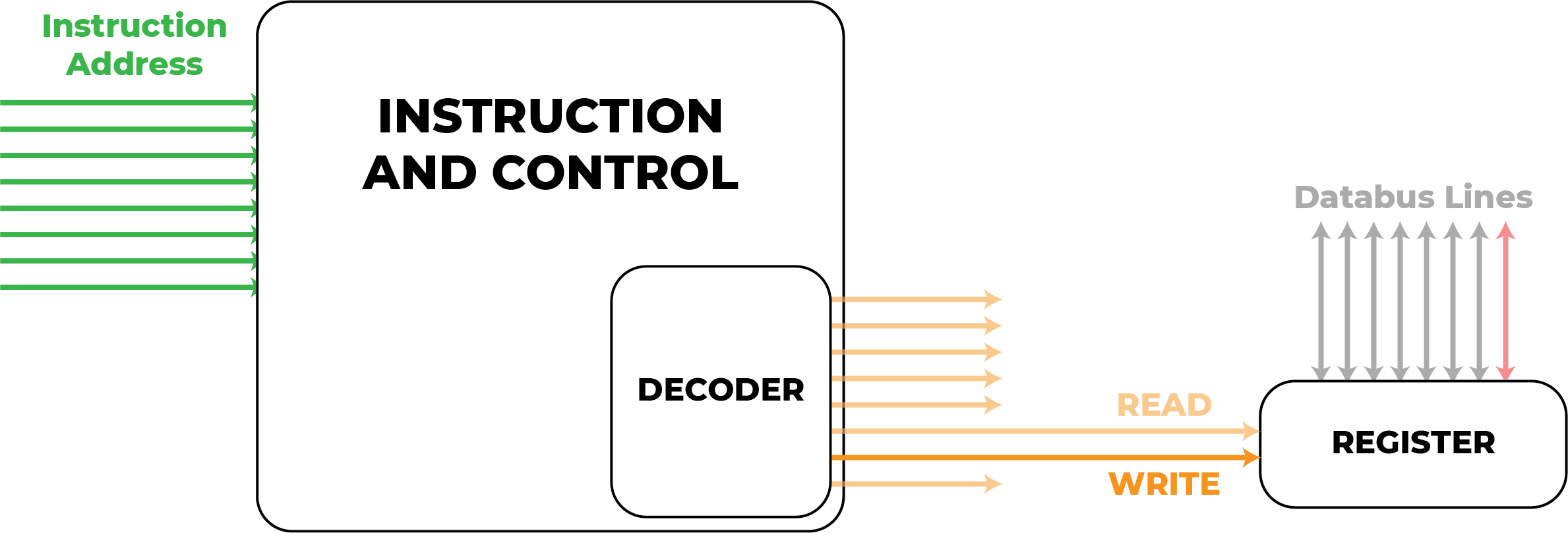
We see the I&C board here, which takes an instruction address, fetches that instruction, and decodes it into a set of control lines. In this simplified case we’re looking at just two of those control signals, a read and a write signal for one of the registers. You’ll also note that the register is connected to the databus and that connection is two-way. The register both can read and write to the databus depending on which control signal is active.
Let’s look at a specific instruction that will load the value \(1\) into register A. In Theoputer Assembly that is the instruction LAI 0x01. For now let’s forget about where the \(1\) comes from and just focus on the register logic:
Note: I’ve colored the first bit of the databus lines red to indicate that the value \(1\) is present on them.
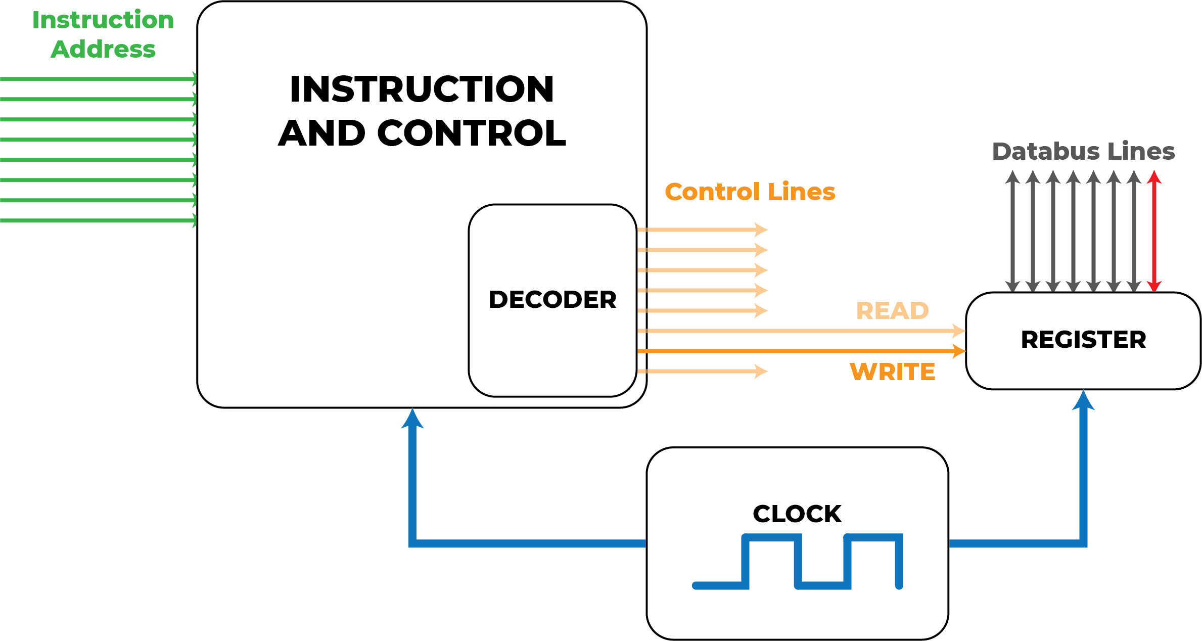
We can see the clock in the drawing now, because something has to tell the decoder and the register to do their respective actions and that is the job of the clock. But we have a problem. We have something called a “race condition” here if we take the diagram at face value.
Off to the Races
Imagine the clock pulses. That pulse takes some amount of time to get
from the clock circuit to the decoder. It appears instantaneous, but
nothing is instantaneous (even quantum leaps, contrary to what you may
have been told). So that pulse takes some time to get to the decoder
and then the decoder takes some time to setup the WRITE control
signal, which takes some time to propagate to the register to tell it
to accept a write operation.
In parallel that original clock pulse is also sent to the register to
tell it to latch the current contents of the databus if and only if
the WRITE signal is active.
But what if the signal to the register’s latch action happens first?! These two paths are racing each other, so we don’t know which one will happen first! There could be thermal noise or capacitances or whatever around that actually delays one of the signals and cause a different path to win seemingly randomly.
At Last, Two Phases
This race condition is the reason for separating out the (fetch + decode) steps from the execute step. We avoid all data race conditions like the one described if we ensure that the control lines get set and then execution happens. The picture really looks like this:
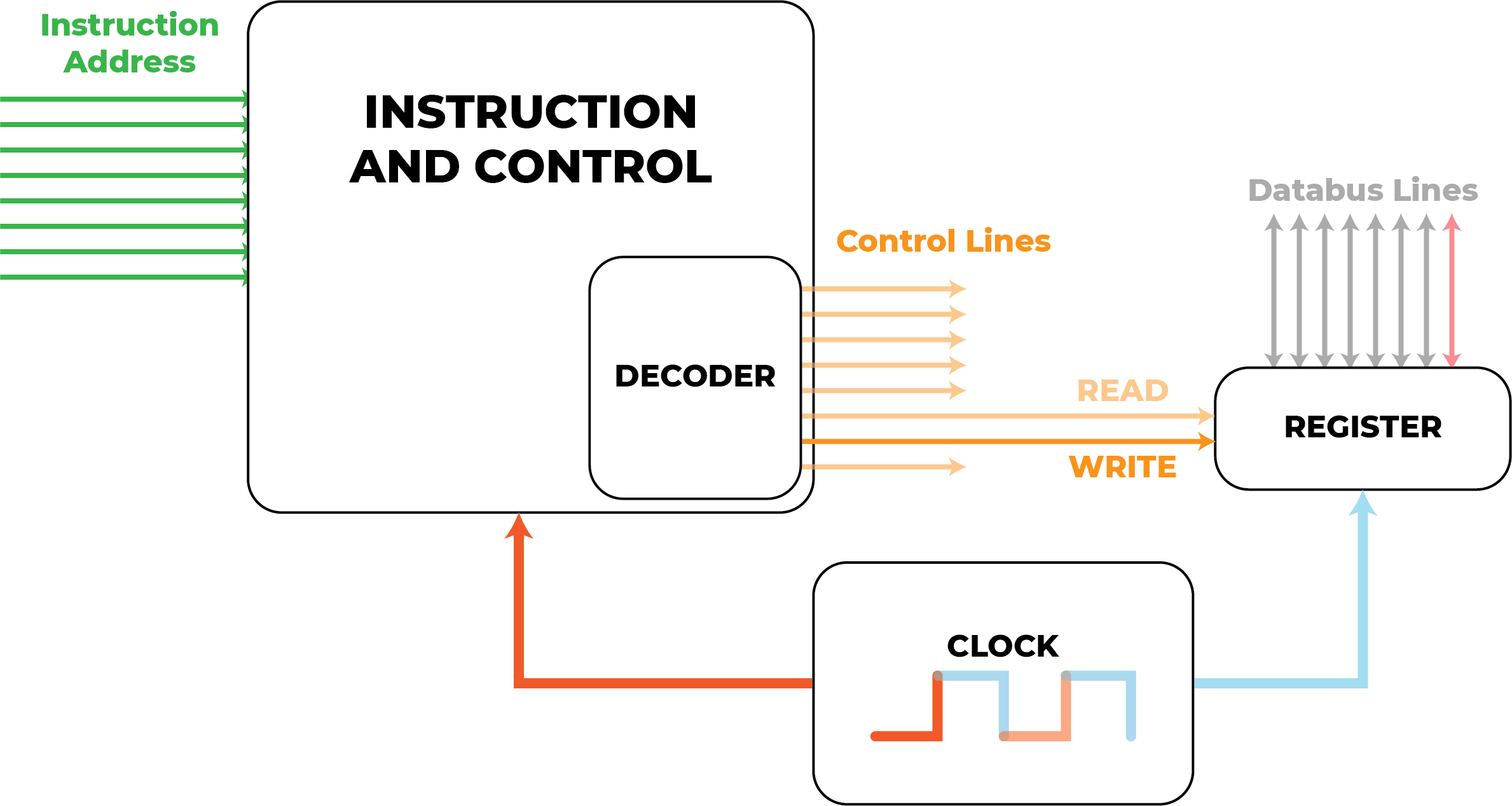
You can see the two phases of the clock now. By convention the (fetch
+ decode) actions happen during the ↓CLK phase and (execute)
actions happen during the ↑CLK phase.
Thus for the rest of the discussion about the Instruction and Control
circuit, we will only discuss things that happen during the (fetch +
decode) / ↓CLK phase.
And You Get a Register!
Everyone gets a register in the Theoputer! In this case the register is going to be critical to several actions. First, let’s consider the complete abstract picture of the LAI 0x01 instruction we looked at before:
If you’ve got your deep engineering hat on you may have a question
about that second execute phase. How are the control lines still set
in that second phase? If the Instruction and Control (I&C) circuit is
intended to only operate during the (fetch + decode) phase, then why
are those control signals not reset as soon as the CLK signal goes
high?
The answer, of course, is that the I&C circuit has some memory inside it so that the control lines are valid throughout the entirety of the (fetch + decode + execute) instruction. If those control lines were somehow allowed to change during the execute phase then we would have all of the same race conditions previously discussed.
The deeper truth here is that the program ROMs will maintain their data outputs until the ROM address changes, which only happens when the Program Counter is changed. So in theory we don’t need this memory. But! It’s good that we added this memory, because when RAM execution entered the picture things got messy enough that the guarantee of instruction data being constant changed.
Of course the word memory should immediately invoke the word register since that’s effectively what memory is: a bank of registers. In this case we give this register a special name: The Instruction Register.
Inside the I&C circuit, the ↓CLK signal actually latches the
Instruction Register, effectively saving the current instruction for
the lifetime of that instruction’s execution phase. Before we look at
the schematic, let’s continue with an abstract view of the LAI
0x01 instruction:
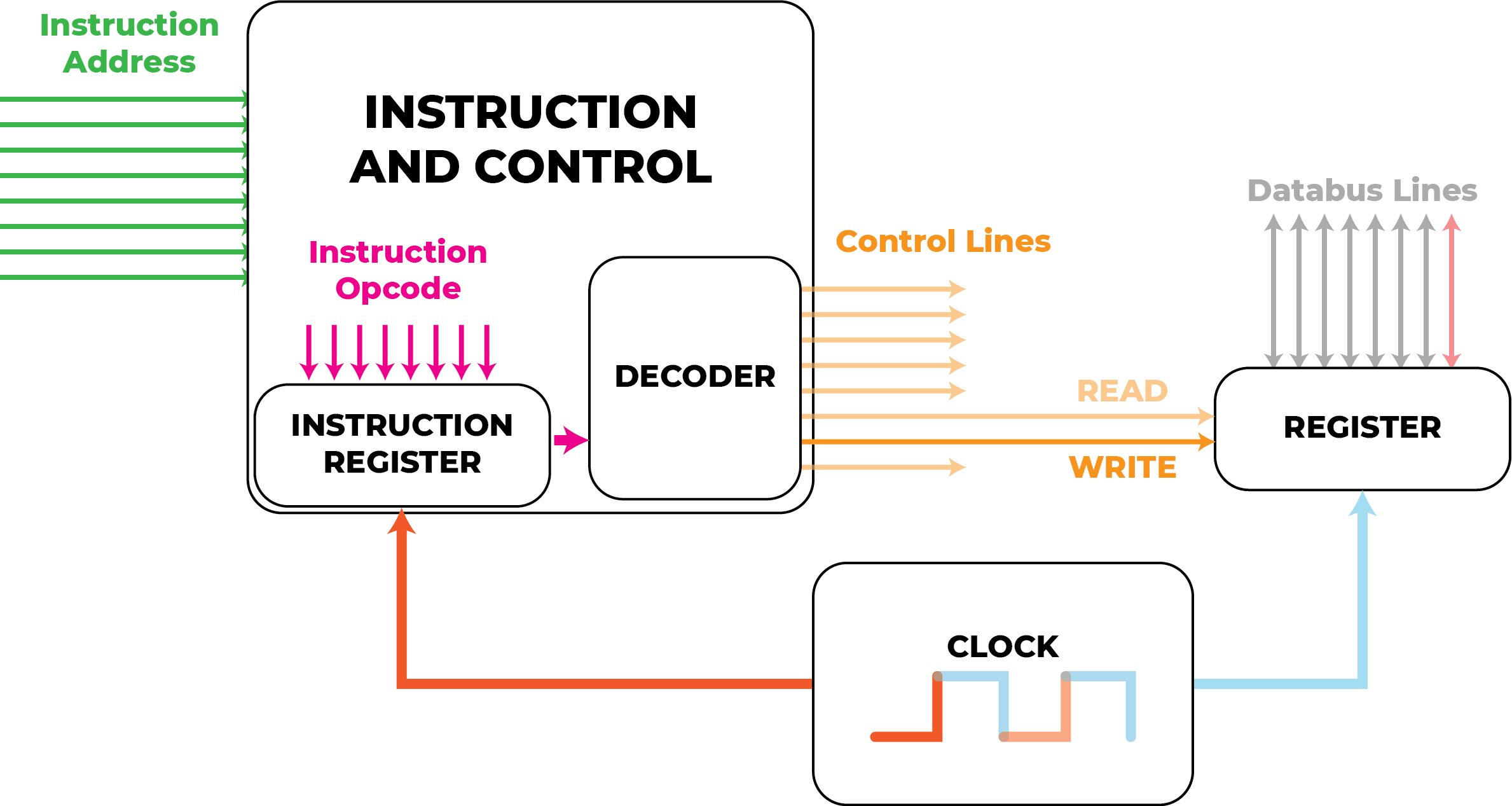
Now we can see that the instruction is saved in the Instruction Register between the two clock phases, ensuring that the control signals remain valid through the entire instruction.
Fetch
Let’s dissect the (fetch + decode) phase by first looking at the fetch. For most of the Theoputer’s life, all instructions were fetched from the program ROMs. That changed recently with a new feature allows instructions to be executed from RAM, but we will avoid that topic here.
Recall that the Program Counter is 16-bits wide. Also recall that all instructions are 16-bits long. These two lengths are not correlated. They just happen to both be 16-bits. Before we dig deeper into the details we first need to define a useful term: Opcode. An opcode is the actual bit sequence of an instruction.
Let’s consider the instruction ADD. In the ISA the ADD operation does the following:
$$ \textrm{REG}_X = \textrm{REG}_A + \textrm{REG}_B $$The opcode for this instruction is:
| Bit 16 | Bit 15 | Bit 14 | Bit 13 | Bit 12 | Bit 11 | Bit 10 | Bit 9 | Bit 8 | Bit 7 | Bit 6 | Bit 5 | Bit 4 | Bit 3 | Bit 2 | Bit 1 |
|---|---|---|---|---|---|---|---|---|---|---|---|---|---|---|---|
| 0 | 1 | 0 | 1 | 0 | 0 | 0 | 1 | 0 | 0 | 0 | 0 | 0 | 0 | 0 | 0 |
Notice that the bottom 8 bits are all zero. This is not coincidental. All of the Theoputer opcodes are actually 8-bits long, with the bottom 8 bits reserved for instruction data (see below).
We could have created variable-length instructions, but there’s not much gain in doing so. This is because of the way ROM works in the Instruction and Control board. The ROM chips in the Theoputer are these awesome ICs from Mircochip: SST39SF010. While they are awesome, they only have 8 data lines. In order to store 16-bit length opcodes, we need two of them!
Sure, we could use one and try to load the first half of the opcode and then load the second one. But that is far more complicated to orchestrate. Throw chips at the problem!
This is a case of good engineering. We don’t need a perfectly designed system right now. There’s enough complexity in the Theoputer as-is. We don’t gain enough by adding in the extra complexity of a system that needs to store parts of opcodes and all of the timing that comes with that. The juice is not worth the squeeze, and if it really ended up mattering we could switch to something more complicated only after we got the simpler system working.
The fetch part of the Instruction and Control board isn’t much more than just two of those SST39SF010 ROM chips wired in parallel so they provide the 16-bit opcode at the input address:
You can ignore the ROM_WE and DISABLE_ROM signals for
now. The ADDR{0-15} lines are connected to the
Program Counter output in the
Daughter Board. This happens via
16 pins attached to the Instruction and Control board that plug into
16 pins on the Daughter Board that connect to the 16 output signals of
the Program Counter.
Instruction Data
Let’s think a bit more critically about the beloved LAI 0x01 instruction. We glossed over where the \(1\) comes from before, but now is a good time to reconsider that glossiness.
Without going through the details of all of the opcodes in the Theoputer (discussed in the post about Theoputer Assembly), let’s look at the opcode for LAI ${value}:
| Bit 16 | Bit 15 | Bit 14 | Bit 13 | Bit 12 | Bit 11 | Bit 10 | Bit 9 | Bit 8 | Bit 7 | Bit 6 | Bit 5 | Bit 4 | Bit 3 | Bit 2 | Bit 1 |
|---|---|---|---|---|---|---|---|---|---|---|---|---|---|---|---|
| 0 | 1 | 1 | 0 | 0 | 0 | 0 | 0 | I08 | I07 | I06 | I05 | I04 | I03 | I02 | I01 |
Those last 8 bits are not numbers. They are arguments to the opcode \(01100000\) and they are intended to be output to the databus from the instruction itself. This enables the programmer to set register A to an arbitrary immediate value as long as it is only 8 bits.
Note: The I in LAI stands for immediate
Recall that in a write-like operation, the register latches the value on the databus. So if we want the immediate value in the instruction itself to wind up in the register, we need to output the last 8 bits of the instruction to the databus.
This is exactly what happens in the Theoputer. This is the schematic for this particular mechanism in the Instruction and Control circuit:
Note: The registers in the Theoputer are all 8 bit and the instruction opcodes are all 16 bit, so there are actually two Instruction Registers. The one pictured above is just the bottom 8 bits.
Here you see the bottom 8 bits of the instruction (INSTR{0-7})
coming in to the bottom 8 bits of the Instruction Register. You can
also see there is a buffer that will output those bottom 8 bits to a
set of lines IR_OUT{0-7} if the signal IO is active. As long
as we connect IR_OUT{0-7} to DBUS{0-7} on the
Daughter Board and connect up the
correct control signal to IO we will get the desired behavior
(spoiler alert: that’s how it’s connected in the Theoputer).
There are several types of instructions that take these kinds of 8-bit parameters:
- Instructions that put an immediate values into a register
- Instructions that copy data to memory locations
- Jump instructions
Most of those instructions also come in flavors that take their parameters from other registers, or memory, or anything that can write the databus in lieu of the parameters. But that’s starting to get into too many of the details of the ISA.
If you prefer the more abstract view of things, this is equivalent to ensuring one of the control lines is connected to the instruction register’s output buffer, which in turn is connected to the databus:
I’ve added in the ROM chip here as well just for some extra clarity.
Long-Argument Instructions
We are dipping our toe slightly into the territory of the decoding part of the Instruction and Control circuit (covered in a separate post), but the Instruction Register is important to understand in the context of the fetch, and thus instruction data is also relevant. Also also it makes sense to discuss the only other feature of instruction data: long argument instructions.
This is a feature that’s been around since the first real ISA, which was ISA V2.0. You probably, rightly, thought that having jumps and memory addresses that can only be 8-bits long is rather limiting. After all, both RAM and ROM have 16-bits of address space.
But we only have 16-bits total for opcode, and the top 8 bits are already claimed to decode the opcode to the control signals. What to do?
The solution in the Theoputer is to have a special bit to indicate that the opcode is a short opcode, and thus the argument is longer. This bit is the most significant bit (MSB) in the opcode (bit 16). If it is \(1\), then only the top 4-bits are used for the actual instruction, allowing for 12-bits of data.
Take, for example, the instruction LAM 0x${address}. This is the instruction to load register A with the contents of RAM at address ${address}. Here is the full 16-bit opcode:
| Bit 16 | Bit 15 | Bit 14 | Bit 13 | Bit 12 | Bit 11 | Bit 10 | Bit 9 | Bit 8 | Bit 7 | Bit 6 | Bit 5 | Bit 4 | Bit 3 | Bit 2 | Bit 1 |
|---|---|---|---|---|---|---|---|---|---|---|---|---|---|---|---|
| 1 | 1 | 0 | 1 | A12 | A11 | A10 | A09 | A08 | A07 | A06 | A05 | A04 | A03 | A02 | A01 |
And in the circuit for the Instruction Register you can see how this MSB is used to control whether the bottom 8 bits or 12 bits are output to the databus:
You’ll note that the path through the bottom buffer there is not actually from a register! Until RAM execution was added the instructions coming from the program ROMs where valid throughout the lifetime of the instruction. Thus we didn’t strictly need any instruction registers.
Writing this blog post actually helped me think through this and fix this problem before production! I’ll take that as a win.
Final Note
All of this business with variable-length arguments seems a little too clever. And that’s a violation of the motto Never Be Clever. In fact, in more modern versions of the Theoputer, there are additional instructions (e.g. JPP) that use the values in the A and B CPU registers to perform jumps and memory address operations. Since each register is 8-bits long, together A and B allow for the full 16-bit parameters needed to address the entirety of the system’s ROM or RAM.
This is especially true for the assembly output of the Cish compiler, which can’t reliably know if 8 or 12 bits is enough. Still, the 8-bit and 12-bit parameterized jumps and memory accessors are faster and thus stick around for the truly clock cycle cutters out there.
What’s Left: Decode
This post is getting quite long and the decode portion of the Instruction and Control circuit/board is quite complicated because the Theoputer uses microinstructions. In an effort to make things more readable, there is a second post dedicated to the decode step.
If for some reason you’re here to see the Instruction and Control board in action, enjoy this fairly long video of the first ever instruction to be fetched and decoded, before the Daughter Board was even built:
There’s a short dedicated post about this video if you prefer to read versus watch.