Introduction
Even the most random memories are useful, some say. Hopefully that’s the case in the Theoputer’s Random Access Memory (RAM) as well.
RAM is often differentiated from other places data is stored along two dimensions:
- It’s faster and smaller than long-term, non-volatile storage (e.g. hard drives)
- It’s slower and larger than registers
To say that RAM is volatile is to say that it requires constant power to stay valid. This is not the case with something like a magnetic drive, where the little magnetic poles can stay in whatever state they were set for a very long time without power. Solid-state drives extend this idea (with A LOT more complexity) to storing information, powerless, for a long time in semiconductors.
But RAM is almost always volatile. In theory in the modern world you could use non-volatile chips like a FRAM to store data without power, but that would be cost-prohibitive. It’s far more appropriate to let the hard drives do their job (storing data that needs to be outlast the power cycle) and let the RAM do its job (store data while the computer is running).
The Theoputer’s RAM is akin to normal RAM, but in complete truth the RAM chip for the Theoputer (IS61C6416AL-12TLI) is fast enough to run at the same speed as the rest of the computer so we could actually use it for registers.
I opted against this because at some point the computer may get fast enough that this is important and because it would be much harder to debug the contents of memory than it is to debug the contents of the registers.
Addressing the RAM
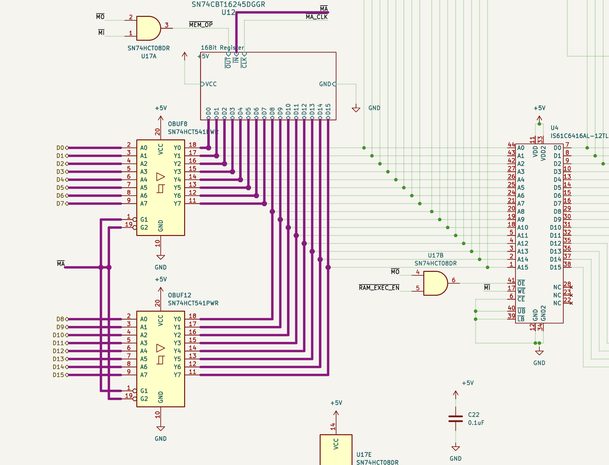
Here is the schematic of the RAM interface, which itself (along with the RAM) is part of the daughter board:
The gates and the JK flip-flop are there to help coordinate the handoff between executing instructions from ROM (the default) to executing them from RAM. There is a dedicated post to that upgrade as well, describing how the Theoputer executes RAM instructions.
Ignoring for now the gates at that JK flip-flop, let’s look
specifically at the four control signals (MA, MI,
MO, CLK) and the 16 bit databus lines (DBUS{0-15}):
MA: Indicates that we want to write to the memory address registerMI: Indicates that we want to write to memoryMO: Indicates that we want to read from memoryCLK: The clock signal to ensure we execute data operations on a↑CLKtransitionDBUS{0-15}: Data lines for whichever operation (memory address, write data, read data) we’re performing
Let’s talk about that MA signal paired with the 16 databus lines
because it may not be immediately clear why we would need such a
mechanism.
In the schematic above you can see that there is only one set of lines
connecting to the databus (DBUS{0-15}) just like most of the other
systems in the computer. Something different about this system,
however, is that we are not really accessing a single data source but
rather a very large bank of them. In particular, you can think of RAM
in the Theoputer as just an array of registers albeit much slower.
Because we effectively have a bank of registers we can read/write from/to, we need a way to address them. We need to know which register to speak with. Just like all other operations in the Theoputer, the way we want to specify such an address is through the databus lines. Using the databus to set the memory address will allow us to control that address via any other part of the system that can write to the databus lines like the actual registers.
But this introduces a subtle problem. We cannot simultaneously use the databus lines to hold the memory address and at the same time hold the contents of the read/write memory operation. Thus we need an intermediate storage place to hold the memory address first and then read/write the contents of memory at that address to/from the databus.
In short we need a register to hold the memory address during a memory
operation. In the Theoputer, since the beginning, memory addresses are
16-bit long and thus we need a 16-bit (or two 8-bit registers) that can
be enabled and disabled (MA) independently of the memory
read/write operation signals (MO and MI).
To help make this a bit more concrete, let’s look at the microcode instructions for the memory read operation:
;; CBA: Copy Register B to RAM address stored in Register A
MA, AO
MI, BO
PS
Note: These microcode instructions are not real in the sense that there is no actual assembly language that understands them. They are just demonstrative.
Imagine if we didn’t have this dedicated MA line and also lacked
a memory address register:
;; CBA: Copy Register B to RAM address stored in Register A
AO, MI, BO
PS
Well that’s a problem! We now have two outputs from registers A and B causing bus contention and the circuit will have no way to determine whether the address should come from A or B nor whether the data to be stored in memory should come from A or B. Lots of problems!
A Tour of the Circuit
As we know now, we need a dedicated memory address register to hold the address we want to operate on while we’re performing the operation. Let’s look at the actual schematic of the RAM system:
You can see (maybe if you zoom in) that this setup looks a lot like the register interface except we are dealing with 16-bit values instead of 8-bit values. However, there are some key differences we should discuss.
Memory Address Interface
The right side of the schematic above is the portion that handles the memory address:
There are two (8-bit x 2) buffers that control whether the DBUS
signals will be connected to the 16-bit address register. Notice that
this register is abstracted in the schematic, but it is effectively
just a doubled version of the 8-bit registers in the computer. The memory address buffers are activated by the
MA signal, which also enables the memory address register to
take input from its data lines:
This address will be clocked in on the standard ↑CLK transition,
adhering to the execution phase scheme used in the Theoputer.
Memory Data Interface
With the memory address register data latched we can now perform the
actual memory operation. In the memory operations the MA signal
will be inactive (i.e. high) and either the MO or MI
signal will be active depending on whether the memory operation is an
output or input respectively.
Let’s consider an output operation, first looking at the address register:
Ahh the fruits of our analysis. Here in the memory operation we are
using the memory address register! The logic gates can get a little
odd in these cases because we are dealing with active low signals, so
let’s look at the AND gate’s truth table that controls the memory
address MEM_OP signal:
| H | H | H |
| H | L | L |
| L | H | L |
| L | L | L |
Long story short, we see that the address register output is only active when one of the memory operation signals is active.
The active MEM_OP signal will cause the lines connected to the
RAM chip’s address inputs to contain the address we want to operate
on! At this point we’ve got a good stable address on the RAM chip, so
let’s look at the right side of the circuit to see the result of the
operation on the data lines:
The D{0-15} pins on the RAM chip are the data pins and are
connected through two buffers to the Theoputer databus DBUS{0-15}
pins. These buffers are fairly unique. Most of the buffers on the
Theoputer are one-way but the ones connected here are actually
bi-directional. That means we can use just two, rather than four, of
them to control the data bits in both input and output operations. If
you look closely, you’ll see the chips here are SN74HCT245PWR’s
instead of the ubiquitous SN74HCT541PWR.
Note: These should probably be HC-type buffers rather than HCT-type buffers. The T indicates these are TTL-level compatible, but at this point in the Theoputer’s existence that interoperability is moot.
The MI line connected to these bi-directional buffers is
highlighted, but not because it’s “active”. The buffers can work in
either direction and this signal dictates which direction they will
buffer to/from. In this case, MI is inactive (high) and that
will cause these SN74HCT245PWR’s to connect the D{0-15} pins
to the DBUS{0-15} pins, and in that direction.
Finally, the MEM_OP signal also appears here and is connected to
the enable pin of the bi-directional buffers so they actually connect
the two sides of the buffer rather than leaving them effectively
disconnected altogether.
The memory input operation works almost identically except the bi-directional buffer direction is flipped causing the databus signals to flow into the memory data pins.
RAM, What is Good For?
The general concept of having a bunch of storage isn’t a wild idea, but it may seem like a lot of extra bits (pun intended) if it’s just going to sit around empty most of the time.
It’s hard to appreciate when just writing assembly how useful RAM can be. Unless you’re an assembly wizard (and you almost assuredly are not a Theoputer assembly wizard), trying to keep a bunch of memory addresses in your head while you program is going to be challenging.
But, the utility of having a large bank of memory becomes painfully apparent when writing in a higher-level language, like Cish. More accurately, it becomes very apparent when writing a C-like compiler. That’s because the RAM starts to become a more integral part of the computer itself once there is the notion of a heap and a stack. If you’re only ever writing assembly, it’s hard to keep track of the complexities of a stack and thus the concept of a stack becomes less useful.
The other valuable thing RAM provides is a fast, modifiable-at-runtime place to execute instructions from. Well, that would be true if the Theoputer could execute instructions from RAM. That turns out to be much harder than it may seem and has its own entire post about how the Theoputer evolved to be able to execute RAM instructions